SIP AND MODULE PARTS
Electric component mounting robots | SiP and module parts
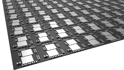
As electronics become smaller with greater functionality and along with demand driving shorter development times, there is an increased demand for package parts such as SiP and module parts. There are many different configurations of package parts that can be found in the market, but the common threads in the manufacturing process of these parts; multi-layering and thinner structures in the Z direction, and higher density in the XY direction, are being used in combination and continue to evolve. For these kinds of cutting-edge processes, Fuji is on hand to talk directly with factories to talk shop and provide an array of solutions.
Contents
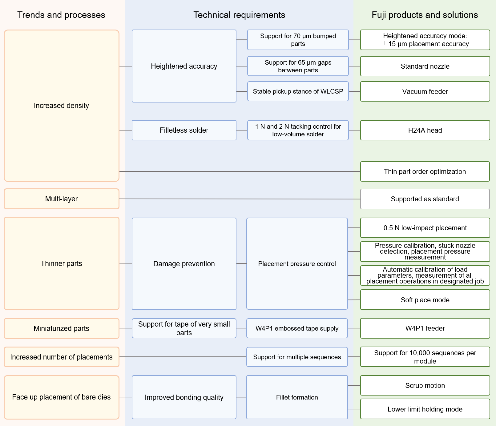
- Placement - Increased density, Thinner parts, Miniaturized parts etc.
- Panel conveyance - Thinner panels, Zero dead space panels etc.
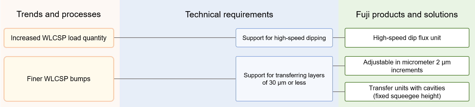
- Transfer process - Increased WLCSP load quantity etc.
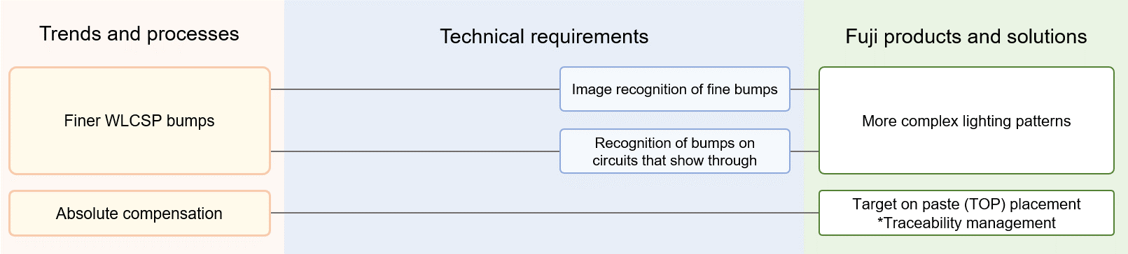
- Vision processing - Finer WLCSP bumps etc.
- Communication - SECS/GEM
Placement
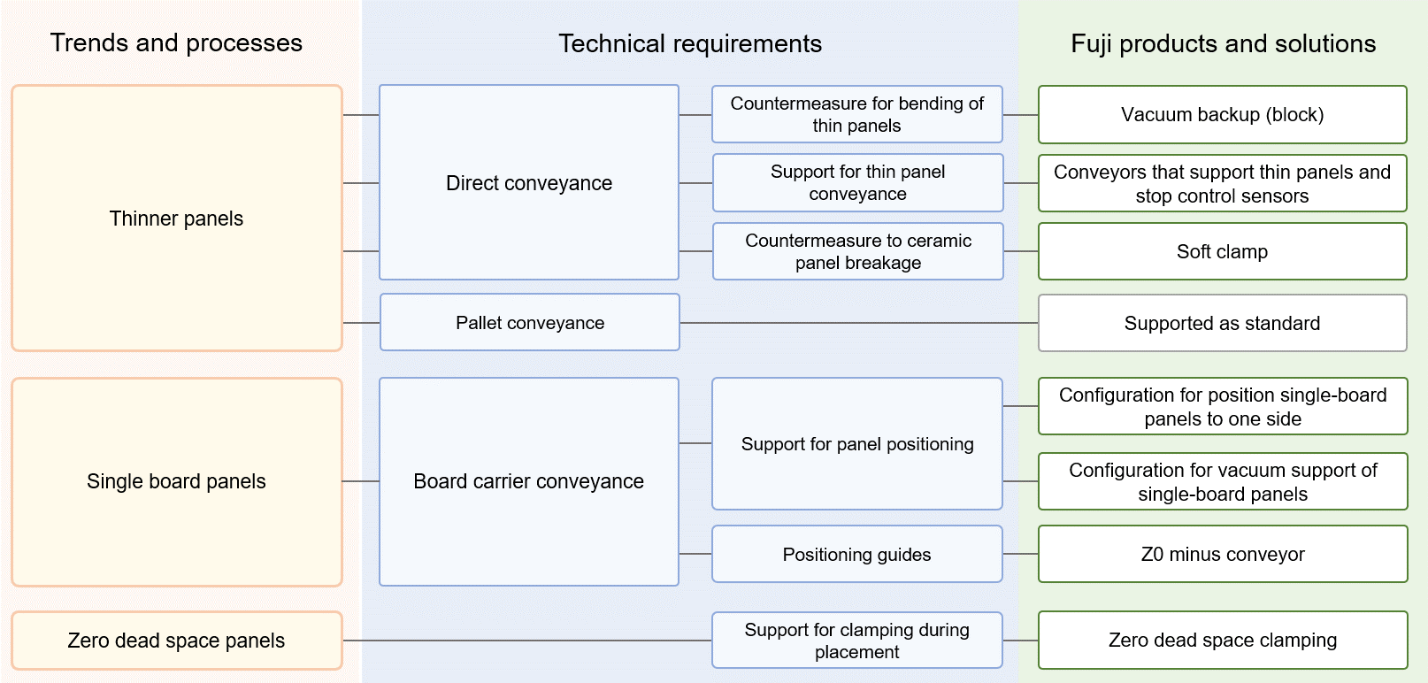
Panel Conveyance
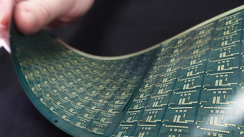
We are able to deliver custom support for conveyance to processes before and after SMT by using methods such as direct conveyance of very thin multiboard panels, pallet conveyance for conveying different types of items, and transporting single-board panels on pallets.
Transfer process
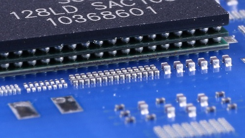
Key devices such as WLCSP are being developed to have smaller bumps, meaning that there is market demand for high-accuracy flux and solder transfer to these smaller bumps. Fuji has the technology for applying thin layers of flux or solder onto parts and improving productivity.
Vision processing
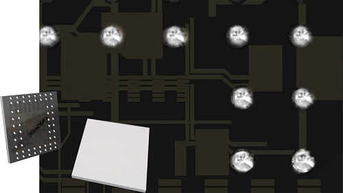
With highly accurate recognition technology driven by our independently developed vision processing camera and LED light source with fine lighting patterns, we are able to support cutting-edge parts that have very small bumps such as WLCSP. We also employ placement correction technology that corrects to the position most advantageous for the effects of self-alignment.
Communication
We comply with the CIM communication software standards that are indispensable for automating semiconductor production lines and comprehensive rules for controlling and communicating with manufacturing equipment.